Common knowledge, yet type "Cerny designed navi" or "Cerny designed RDNA", into Google you get practically no relevant results, and the results you do get just point back to the Road to PS5 video.
What did Cerny say in the video?
"First we have a custom AMD GPU based on their RDNA technology. What does that mean? AMD is continuously improving and revising their tech. For RDNA2 their goals were, roughly speaking, to reduce power consumption by rearchitecting the GPU to put data close to where it's needed. To optimize the GPU for performance and to add a new, more advanced, feature set. But that feature set is malleable. Which is to say that we have our own needs for PlayStation and that can factor into what the AMD roadmap becomes.
Not only does it not state that Cerny designed Navi or RDNA 2, but he specifically calls it AMD's technology. Now I think this is the part you are referring to:
"So collaboration is born.
If we bring concepts to AMD that are felt to be widely useful then they can be adopted into RDNA, and used broadly including in PC GPUs. If the ideas are sufficiently specific to what we're trying to accomplish, like the GPU cache scrubbers I was talking about, then they end up being just for us. If you see a similar discrete GPU available as a PC card at roughly the same time as we release our console that means our collaboration with AMD succeeded.
In producing technology useful in both worlds. It doesn't mean that we as Sony simply incorporated the PC part into our console."
And if we look at the PC space, the 6700 XT looks pretty much like the PS5 GPU, but without some of the custom features, and with the Infinity Cache. So it looks like Cerny was correct in what he said. Navi 22 may well have come out of the collaboration with Sony. That doesn't mean Cerny or Sony designed the RDNA architecture that underlies it. Even if Sony did help develop particular features that made it into RDNA 2, that's not the same as creating an entire architecture. And it doesn't mean that Cerny personally worked on those features, or did the transistor layout himself. Architectures are created by entire teams, not one single person.
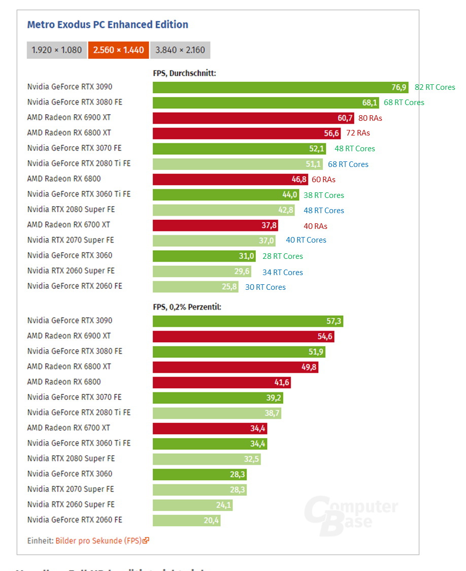
Sure, because rather than adding more SMs (comparing 3080 vs 2080 Ti) Nvidia increased raytracing and FP32 capabilities per SM. If they simply had used the extra transistors to scale the Turing architecture up, we would also expect a big difference in ray tracing performance. The question I think is for a given transistor budget/die size, is Ampere much more performant than Turing? And in that benchmark, you can see the 3070 and 2080 Ti pretty much tied, with the 2080 Ti having ~7% more transistors. The 6700 XT looks to be the closest AMD part in size, and is much slower in ray tracing performance than both.

 it's a common knowledge from awhile. There a Twitter about it of Lisa Su. Now you want the precise minute in the ps5 presentation, it's the part where he talk about the TF number at the beginning, go to watch it, aren't too much comfy isn't it?. Are you really so troll?