-
Hey, guest user. Hope you're enjoying NeoGAF! Have you considered registering for an account? Come join us and add your take to the daily discourse.
You are using an out of date browser. It may not display this or other websites correctly.
You should upgrade or use an alternative browser.
You should upgrade or use an alternative browser.
Possible SSD tech behind PS5 and Scarlet
- Thread starter Shangounchained
- Start date
- Opinion
Could this speed up backwards compatible games too? Or would they need to be programmed for it?
Most certainly not. Apart from faster filesystem (load times, transitions)
Birdo
Banned
Most certainly not. Apart from faster filesystem (load times, transitions)
Aww

Shrap
Member
Whoa. Calm down. You wrote SSD in your title so don't yell at others for your own shortcomings.It's SSG solid state graphics it's actually vram! And according to this demo it's 2terabytes of VRAM so stop the retard reactions!
You know the GDDR5 in a stock PS4? It runs at 176GB/s. Best case scenario this "SSG" tech runs at 8GB/s. Get ready for 2TBs of the world's slowest VRAM.
pr0cs
Member
Dunno, but it REALLY hurt the experience. Happily RDR2 on oneX was fine but the load times of gta5 on ps4 did cross my mind before I pulled the trigger on rdr2Doesn't the PS4 use a 5400rpm hard drive over SATA 2? This is like 2006 level hard drive technology. Even the worst SSD known to man would provide massive speed bumps with regards to loading.
Shangounchained
Banned
the SSG is still an SSD simply soldered to the GPU cutting latencies and the reason it acts like vram is if the GPU tries to stream assets on the gddr6 and aren't available then it can go straight to the SSG which is faster than your usual SSD, like the demo shown hereWhoa. Calm down. You wrote SSD in your title so don't yell at others for your own shortcomings.
You know the GDDR5 in a stock PS4? It runs at 176GB/s. Best case scenario this "SSG" tech runs at 8GB/s. Get ready for 2TBs of the world's slowest VRAM.

That frame onscreen here is 250 billion polygons you can't render this frame on any consumer card call it gtx titan rtx titan or 2080tis you'll need a rack of gtx titans to render quarters of the frame to pull this, it's only possible because of the SSG, doesn't matter how slow it is but the capacity allows for it to render such a complex frame,
You can have a GPU with 2 million GB/s but with 8gb of vram you won't dream of rendering this frame!
Komatsu
Member
Wait, are we talking VRAM here? What does this have to do with the solid state drives that both major nextgen consoles will supposedly have?
As for using HBM, it doesn't surprise me in the least, as space always comes at a premium. It'll provide performance with lower power consumption, (potentially) much higher bandwidth and it will not be as taxing on the console's "heat budget".
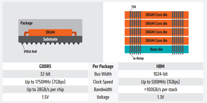
This is all blackboard stuff, of course. In reality, I've done some work with the Radeon VII (which is a HBM2 offering from AMD) and it ran hotter, slower and consumed more power than the RTX 2080. So we'll see how their HBM component in their nextgen APU will fare.
As for using HBM, it doesn't surprise me in the least, as space always comes at a premium. It'll provide performance with lower power consumption, (potentially) much higher bandwidth and it will not be as taxing on the console's "heat budget".
This is all blackboard stuff, of course. In reality, I've done some work with the Radeon VII (which is a HBM2 offering from AMD) and it ran hotter, slower and consumed more power than the RTX 2080. So we'll see how their HBM component in their nextgen APU will fare.
Kenpachii
Member
the SSG is still an SSD simply soldered to the GPU cutting latencies and the reason it acts like vram is if the GPU tries to stream assets on the gddr6 and aren't available then it can go straight to the SSG which is faster than your usual SSD, like the demo shown here
That frame onscreen here is 250 billion polygons you can't render this frame on any consumer card call it gtx titan rtx titan or 2080tis you'll need a rack of gtx titans to render quarters of the frame to pull this, it's only possible because of the SSG, doesn't matter how slow it is but the capacity allows for it to render such a complex frame,
You can have a GPU with 2 million GB/s but with 8gb of vram you won't dream of rendering this frame!
Then why even put expensive gddr6 at this point in that box?
Last edited:
Shangounchained
Banned
Go watch the demo and read the article, don't just jump on a moving train! You need the gddr6 for obvious reason it's vram but if u rub out of room on that vram you can quickly switch to the ssGThen why even put expensive gddr6 at this point in that box?
Shangounchained
Banned
Go read the article before commenting it's SSG solid state graphics and it's 2 terabytes of it all vramWait, are we talking VRAM here? What does this have to do with the solid state drives that both major nextgen consoles will supposedly have?
As for using HBM, it doesn't surprise me in the least, as space always comes at a premium. It'll provide performance with lower power consumption, (potentially) much higher bandwidth and it will not be as taxing on the console's "heat budget".
This is all blackboard stuff, of course. In reality, I've done some work with the Radeon VII (which is a HBM2 offering from AMD) and it ran hotter, slower and consumed more power than the RTX 2080. So we'll see how their HBM component in their nextgen APU will fare.
Negotiator
Member
Because you need it for the framebuffer.Then why even put expensive gddr6 at this point in that box?
Because you need it for the framebuffer.
Or any render-target.
thicc_girls_are_teh_best
Member
All the endurance talk is moot if the pages will be writable by OS only. And marked read-only for games.
And it will be the case because filesystem will be mapped to the same pages anyway.
Endurance isn't a moot point; the data still has to be written to the chips. However fast it can be written doesn't suddenly mean the wear level on the cells in the chips somehow becomes more tolerant: a write is a write.
Switching it to read-only for games means the controller would have to switch it back to write-enable mode when more data needs to be written to the NAND. All that said, we don't know what efforts Sony and MS are taking to cut down on wear leveling and things of that nature. And P/E cycles ultimately don't mean too much if data isn't being written super-frequently (which if these were server systems or systems being used for things like video production, would be the case).
That said, there's really not much to their SSD talk other than PCIe 4.0 connections; the person bringing up SSG, I don't know how that would work in a console where the GPU and CPU are integrated in an APU. I'm guessing the GPU portion would just have a built-in flash memory controller for the NAND? But then would the GPU just shift "older" data out of the GDDR6 to the onboard NAND similar to the way CPUs move older data out of SRAM caches to DRAM? Would the GPU have a microcontroller built in to handle that automatically so that the CPU doesn't need to waste cycles doing that for the GPU?
It's all rather interesting to consider and I think seeing it that way, maybe the talk of this "SSD cache" the way it's being trickled out by Sony and MS could be pretty unique and not something we're seeing on PC at the moment. Even if it is still using conventional NAND over pseudo-DRAM NAND.
Shangounchained
Banned
So you mean to say AMD are sooooo stupid to put a nand ssd on that SSG card for professional workstations?Endurance isn't a moot point; the data still has to be written to the chips. However fast it can be written doesn't suddenly mean the wear level on the cells in the chips somehow becomes more tolerant: a write is a write.
Switching it to read-only for games means the controller would have to switch it back to write-enable mode when more data needs to be written to the NAND. All that said, we don't know what efforts Sony and MS are taking to cut down on wear leveling and things of that nature. And P/E cycles ultimately don't mean too much if data isn't being written super-frequently (which if these were server systems or systems being used for things like video production, would be the case).
That said, there's really not much to their SSD talk other than PCIe 4.0 connections; the person bringing up SSG, I don't know how that would work in a console where the GPU and CPU are integrated in an APU. I'm guessing the GPU portion would just have a built-in flash memory controller for the NAND? But then would the GPU just shift "older" data out of the GDDR6 to the onboard NAND similar to the way CPUs move older data out of SRAM caches to DRAM? Would the GPU have a microcontroller built in to handle that automatically so that the CPU doesn't need to waste cycles doing that for the GPU?
It's all rather interesting to consider and I think seeing it that way, maybe the talk of this "SSD cache" the way it's being trickled out by Sony and MS could be pretty unique and not something we're seeing on PC at the moment. Even if it is still using conventional NAND over pseudo-DRAM NAND.
Shangounchained
Banned
Read the article, and it's not using pcie 4.0 or whatsoeverEndurance isn't a moot point; the data still has to be written to the chips. However fast it can be written doesn't suddenly mean the wear level on the cells in the chips somehow becomes more tolerant: a write is a write.
Switching it to read-only for games means the controller would have to switch it back to write-enable mode when more data needs to be written to the NAND. All that said, we don't know what efforts Sony and MS are taking to cut down on wear leveling and things of that nature. And P/E cycles ultimately don't mean too much if data isn't being written super-frequently (which if these were server systems or systems being used for things like video production, would be the case).
That said, there's really not much to their SSD talk other than PCIe 4.0 connections; the person bringing up SSG, I don't know how that would work in a console where the GPU and CPU are integrated in an APU. I'm guessing the GPU portion would just have a built-in flash memory controller for the NAND? But then would the GPU just shift "older" data out of the GDDR6 to the onboard NAND similar to the way CPUs move older data out of SRAM caches to DRAM? Would the GPU have a microcontroller built in to handle that automatically so that the CPU doesn't need to waste cycles doing that for the GPU?
It's all rather interesting to consider and I think seeing it that way, maybe the talk of this "SSD cache" the way it's being trickled out by Sony and MS could be pretty unique and not something we're seeing on PC at the moment. Even if it is still using conventional NAND over pseudo-DRAM NAND.
Last edited:
Von Hugh
Member
Read the article, and it's not using pcie 4.0 or whatsoever
Don't reply twice to the same post. Jesus Christ.
Maybe you should read the post you are replying to first.
Endurance isn't a moot point; the data still has to be written to the chips. However fast it can be written doesn't suddenly mean the wear level on the cells in the chips somehow becomes more tolerant: a write is a write.
Switching it to read-only for games means the controller would have to switch it back to write-enable mode when more data needs to be written to the NAND. All that said, we don't know what efforts Sony and MS are taking to cut down on wear leveling and things of that nature. And P/E cycles ultimately don't mean too much if data isn't being written super-frequently (which if these were server systems or systems being used for things like video production, would be the case).
That said, there's really not much to their SSD talk other than PCIe 4.0 connections; the person bringing up SSG, I don't know how that would work in a console where the GPU and CPU are integrated in an APU. I'm guessing the GPU portion would just have a built-in flash memory controller for the NAND? But then would the GPU just shift "older" data out of the GDDR6 to the onboard NAND similar to the way CPUs move older data out of SRAM caches to DRAM? Would the GPU have a microcontroller built in to handle that automatically so that the CPU doesn't need to waste cycles doing that for the GPU?
It's all rather interesting to consider and I think seeing it that way, maybe the talk of this "SSD cache" the way it's being trickled out by Sony and MS could be pretty unique and not something we're seeing on PC at the moment. Even if it is still using conventional NAND over pseudo-DRAM NAND.
Managing writes is what flash controllers do. In all ssd drives. It's not a problem.
If flash controller maps all flash as a memory page and also gives a filesystem interface over it, it will behave very much like ssd, but low latency and high bandwidth.
Now you arrange a streaming buffer for assets in gddr and then stream these assets there. Another possibility would be to use flash controller directly for texture fetches and other relatively infrequent per frame data. The most of the gddr bandwidth consumed by rops when rendering into various targets. If you don't use flash as render target I would say even 2gb/sec is enough.
Dontero
Banned
What prevents AMD from using flash memory for texture data? It's read-only and is cached in tex store units for fast access anyway.
Bandwidth. When you talk about GDDR you talk about 100s of GB/s not few GB/s (and only for big files, for small files you are looking at few dozens to 100s of MB/s not GB/s)
And this is old tech. They will probably want to use something like HBM2 which can go to even 2TB/s aka 2000Gb/s for graphics memory.
It's SSG did you even read! It's not your typical ssd it's a ssd soldered directly to the GPU and it's accessible directly to the GPU it acts more like vram, and there's a demo of it showcasing a data set of 250 billion polygons on a scene this is an impossible feat for any consumer card out there!
SSG is nice for video editing and not that much for gaming because even if you attach it to GPU you won't be able to speed it up to VRAM bandwidth which is NEEEDED. Sure you can make huge level but that level also needs to be rendered which means no performance. So great for CAD and offline rendering not so much for real time rendering which is what games do.
Last edited:
Bandwidth. When you talk about GDDR you talk about 100s of GB/s not few GB/s (and only for big files, for small files you are looking at few dozens to 100s of MB/s not GB/s)
And this is old tech. They will probably want to use something like HBM2 which can go to even 2TB/s aka 2000Gb/s for graphics memory.
SSG is nice for video editing and not that much for gaming because even if you attach it to GPU you won't be able to speed it up to VRAM bandwidth which is NEEEDED. Sure you can make huge level but that level also needs to be rendered which means no performance. So great for CAD and offline rendering not so much for real time rendering which is what games do.
Bandwidth is needed for render targets. Texture fetches are cached.
Shangounchained
Banned
This is the only implementation better for gaming because it uses it as vram and even though having the gddr6 vram with it, let's wait and see how they'll demonstrate it on ps5 currently it's about load times but there's more to it than loading! I mean that frame had 250 billion polygons do you know what that means, simply means no card out there can do it no titan no rtx only a combination of ssd and hbm or gddr can pull this outBandwidth. When you talk about GDDR you talk about 100s of GB/s not few GB/s (and only for big files, for small files you are looking at few dozens to 100s of MB/s not GB/s)
And this is old tech. They will probably want to use something like HBM2 which can go to even 2TB/s aka 2000Gb/s for graphics memory.
SSG is nice for video editing and not that much for gaming because even if you attach it to GPU you won't be able to speed it up to VRAM bandwidth which is NEEEDED. Sure you can make huge level but that level also needs to be rendered which means no performance. So great for CAD and offline rendering not so much for real time rendering which is what games do.
Shangounchained
Banned
It's not your casual ssd it's SSD vramI will be kinda angry if ps5 and next xbox will have these amazing load times with a simple ssd/nvme while my 2k usd new pc with nvme drives will probably not be as fast
The SSD feature makes me really excited about all of this. When games are programmed with SSDs in mind you can archive so much more. And not only because of loadtimes but also performance
Digital Foundry has a video showing how Star Citizen basically needs a SSD to be playable.
this is true next gen and a real evolution. For the first time games will be programmed with this in mind.
Digital Foundry has a video showing how Star Citizen basically needs a SSD to be playable.
this is true next gen and a real evolution. For the first time games will be programmed with this in mind.
Last edited:
Shangounchained
Banned
The SSD feature makes me really excited about all of this. When games are programmed with SSDs in mind you can archive so much more. And not only because of loadtimes but also performance
Digital Foundry has a video showing how Star Citizen basically needs a SSD to be playable.
this is true next gen and a real evolution. For the first time games will be programmed with this in mind.
It's not this kind of ssd implementation, the implementation on the article is about SSG solid state graphics go read it, it's an SSD used as vram directly accessible from the GPU
ScaryBrandon
Banned
Its just an nvme ssd dude get over it. No console has ever broken new grounds, its always old pc tech with a lot of marketing buzzwords.
Last edited:
Shangounchained
Banned
Your talking shit!Its just an nvme ssd dude get over it. No console has ever broken new grounds, its always old pc tech with a lot of marketing buzzwords.
Negotiator
Member
Basically what Wii U did with the slow DDR3 (textures) + very fast eDRAM (framebuffer/render-target) setup.Another possibility would be to use flash controller directly for texture fetches and other relatively infrequent per frame data. The most of the gddr bandwidth consumed by rops when rendering into various targets. If you don't use flash as render target I would say even 2gb/sec is enough.
Btw, how will next-gen games handle game saves if the SSD is marked read-only for them?
flacopol
Member
I hope it's improved because many of the console games I abandon now are simply due to load times (looking at you gta5)
Every time I see AGDQ , love to see the bloodborne run... until I see more loading that playing... even with a SSD
Basically what Wii U did with the slow DDR3 (textures) + very fast eDRAM (framebuffer/render-target) setup.
Btw, how will next-gen games handle game saves if the SSD is marked read-only for them?
The memory interface can be read only. While filesystem layer is writable.
Filesystem will use open/read/write os api anyway.
thicc_girls_are_teh_best
Member
Okay, so now that some things have been cleared up, basically what you guys are saying is that the consoles could just be interfacing the NAND to the GPU directly and use data put there as a texture cache. Which I suppose if just for textures that could work and would be noticeably faster than through PCIe as a storage device like other SSDs.
But there's still some things that don't feel right about it. If the NAND's embedded to the board and interfaced directly with the GPU, what happens if (when?) the NAND starts slowing down and the endurance levels are reached? The textures still have to be written to NAND in the first place, that's still a write operation. It's still finite in size, and different games will have different amounts of texture data to utilize. A player could need to install a new game to the drive while they have other games installed there for a while, that kind of facilitates the NAND needing to be set back to write-enable (is there a way to set specific chips to read-only and others to write-enable in the same pool by a memory controller? Genuine question).
And there's a reason I keep bringing up P/E cycles particularly with QLC; they don't have very high P/E ratings and over the course of 5-7 years core and hardcore users are going to be writing a LOT of data to that storage. Optimally you would hope the storage is removable and replaceable in some capacity because of that possibility.
Also, if that same NAND pool's being used for other data unrelated to texture cache, you may now have an issue of that memory and the bandwidth not being used in a fully optimal way i.e using it for save file loads and the save files may only be a few MBs in total (I know certain games have save files as large as 500 MB but those are highly unoptimized for save file sizes, let's be honest xD). You'd ideally want as much of that memory and bandwidth used for as much of that most critical task as possible. But it sounds like Sony and MS's solutions will be using it for all types of data, not just textures or assets bound for GPU compute.
At that point, why not just split that pool and have some set directly to the CPU portion to store non-graphics data? This isn't RAM, there's not going to be any data copying between the different pools.
Look I'm not shitting on the SSG implementation, in fact I think it could work and seems pretty interesting. It also does well with regards to compromises. But it will have a very different use-case with PS5 and Scarlett vs. AMD's server/workstation-orientated cards. That's the kind of stuff I'm trying to keep in mind with my skepticism, that's all.
Shangounchained
Banned
Nobody said ps5 would use nand, it's the Radeon pro SSG that uses nand up to this moment we don't know what kind of ssd the ps5 will go for in this GPU ssd combinationOkay, so now that some things have been cleared up, basically what you guys are saying is that the consoles could just be interfacing the NAND to the GPU directly and use data put there as a texture cache. Which I suppose if just for textures that could work and would be noticeably faster than through PCIe as a storage device like other SSDs.
But there's still some things that don't feel right about it. If the NAND's embedded to the board and interfaced directly with the GPU, what happens if (when?) the NAND starts slowing down and the endurance levels are reached? The textures still have to be written to NAND in the first place, that's still a write operation. It's still finite in size, and different games will have different amounts of texture data to utilize. A player could need to install a new game to the drive while they have other games installed there for a while, that kind of facilitates the NAND needing to be set back to write-enable (is there a way to set specific chips to read-only and others to write-enable in the same pool by a memory controller? Genuine question).
And there's a reason I keep bringing up P/E cycles particularly with QLC; they don't have very high P/E ratings and over the course of 5-7 years core and hardcore users are going to be writing a LOT of data to that storage. Optimally you would hope the storage is removable and replaceable in some capacity because of that possibility.
Also, if that same NAND pool's being used for other data unrelated to texture cache, you may now have an issue of that memory and the bandwidth not being used in a fully optimal way i.e using it for save file loads and the save files may only be a few MBs in total (I know certain games have save files as large as 500 MB but those are highly unoptimized for save file sizes, let's be honest xD). You'd ideally want as much of that memory and bandwidth used for as much of that most critical task as possible. But it sounds like Sony and MS's solutions will be using it for all types of data, not just textures or assets bound for GPU compute.
At that point, why not just split that pool and have some set directly to the CPU portion to store non-graphics data? This isn't RAM, there's not going to be any data copying between the different pools.
Look I'm not shitting on the SSG implementation, in fact I think it could work and seems pretty interesting. It also does well with regards to compromises. But it will have a very different use-case with PS5 and Scarlett vs. AMD's server/workstation-orientated cards. That's the kind of stuff I'm trying to keep in mind with my skepticism, that's all.
thicc_girls_are_teh_best
Member
Nobody said ps5 would use nand, it's the Radeon pro SSG that uses nand up to this moment we don't know what kind of ssd the ps5 will go for in this GPU ssd combination
SSDs and SSG both use NAND. There are primarily four types of NAND: SLC, MLC, TLC and QLC. There is also managed NAND in the form of things such as e-MMC, and EEPROM which is also NAND-based but in read-only memory format and more flexible in use for updates than EPROM or ROM. Then there are NVRAM, which combine NAND benefits with some benefits of DRAM, such as FRAM and MRAM. You also have NOR Flash which is arranged differently from NAND even though both are based on the same underlying technology (it also tends to have much faster read speed but much slower writes, lower capacity, byte-addressable for writes AND reads (DRAM is only page-addressable for reads) and can have up to a 32-bit data bus (NAND tends to go for either 8-bit or 16-bit buses; some SLC NANDs have 32-bit data buses though).
All modern storage devices that aren't platter magnetic disk-based or floppy-based are using some type of conventional NAND, and the NAND being used in AMD's SSG Radeon card is also a type of conventional NAND. It is just networked to the GPU differently than how SSDs interface with a typical system through SATA, SATA Express or NVMe interfaces over a SATA or M.2 connector.
When Sony has been saying SSD in those Wired articles, they are referring to some form of storage using some form of NAND. Whether it is purely conventional NAND, managed NAND, or mixing in some type of NVRAM etc., at the capacities they are hinting at and sizes of storage in previous systems to go by, it is almost 100% guaranteed to be some type of NAND. The only other option they could have aside from what I listed above is 3D Xpoint-style NAND used as pseudo DRAM, similar to Intel's Optane Persistent Memory, but you aren't getting anywhere near 1TB of that in a consumer-level device like a games console, even if it is next-gen. Just would never be price-efficient.
So they would either be referring to some sort of pseudo-DRAM style NAND (already said why this probably won't be the case), or more conventional 3D NAND/QLC NAND networked to the GPU providing perhaps a texture cache like what the AMD product likely does (though I suspect that product IS using pseudo-DRAM style NAND, i.e 3D Xpoint, if it costs multiple hundreds or even thousands of dollars like Intel's Optane Persistent Memory does).
A SSG-style setup using TLC or QLC NAND in place of pseudo-DRAM style NAND to get big capacities (1TB minimum) networked to the GPU directly as a texture cache and (maybe) using some DDR3/DDR4 as a faster, smaller cache pool seems the most probable. It can keep the prices down (QLC is not expensive to buy in bulk at notable capacities; Sony and MS would get it for even cheaper), still provide great speeds (between 2-8GB/s, depends on how it's interfaced), and can keep the system in line with BOM budget. Better still, users can still use a secondary drive if they want, to store additional files, which would be removable, but probably act more like a conventional SSD over some type of M.2 interface (probably at 1/2 the speed of the SSG solution).
I'll be very surprised if Sony or Microsoft pull out something that hasn't already been mentioned here; tech like MRAM and FRAM are still way too high for too little capacity, and others like NRAM are only just finding technology partners to produce the chips. Most of these are untested in mass-market devices and I doubt Sony or MS would take a chance on these for gaming platforms to the scale of their upcoming ones.
Last edited:
Shangounchained
Banned
Coul
could be using resistive ram a.k.a RERAM! there's rumours about thisSSDs and SSG both use NAND. There are primarily four types of NAND: SLC, MLC, TLC and QLC. There is also managed NAND in the form of things such as e-MMC, and EEPROM which is also NAND-based but in read-only memory format and more flexible in use for updates than EPROM or ROM. Then there are NVRAM, which combine NAND benefits with some benefits of DRAM, such as FRAM and MRAM. You also have NOR Flash which is arranged differently from NAND even though both are based on the same underlying technology (it also tends to have much faster read speed but much slower writes, lower capacity, byte-addressable for writes AND reads (DRAM is only page-addressable for reads) and can have up to a 32-bit data bus (NAND tends to go for either 8-bit or 16-bit buses; some SLC NANDs have 32-bit data buses though).
All modern storage devices that aren't platter magnetic disk-based or floppy-based are using some type of conventional NAND, and the NAND being used in AMD's SSG Radeon card is also a type of conventional NAND. It is just networked to the GPU differently than how SSDs interface with a typical system through SATA, SATA Express or NVMe interfaces over a SATA or M.2 connector.
When Sony has been saying SSD in those Wired articles, they are referring to some form of storage using some form of NAND. Whether it is purely conventional NAND, managed NAND, or mixing in some type of NVRAM etc., at the capacities they are hinting at and sizes of storage in previous systems to go by, it is almost 100% guaranteed to be some type of NAND. The only other option they could have aside from what I listed above is 3D Xpoint-style NAND used as pseudo DRAM, similar to Intel's Optane Persistent Memory, but you aren't getting anywhere near 1TB of that in a consumer-level device like a games console, even if it is next-gen. Just would never be price-efficient.
So they would either be referring to some sort of pseudo-DRAM style NAND (already said why this probably won't be the case), or more conventional 3D NAND/QLC NAND networked to the GPU providing perhaps a texture cache like what the AMD product likely does (though I suspect that product IS using pseudo-DRAM style NAND, i.e 3D Xpoint, if it costs multiple hundreds or even thousands of dollars like Intel's Optane Persistent Memory does).
A SSG-style setup using TLC or QLC NAND in place of pseudo-DRAM style NAND to get big capacities (1TB minimum) networked to the GPU directly as a texture cache and (maybe) using some DDR3/DDR4 as a faster, smaller cache pool seems the most probable. It can keep the prices down (QLC is not expensive to buy in bulk at notable capacities; Sony and MS would get it for even cheaper), still provide great speeds (between 2-8GB/s, depends on how it's interfaced), and can keep the system in line with BOM budget. Better still, users can still use a secondary drive if they want, to store additional files, which would be removable, but probably act more like a conventional SSD over some type of M.2 interface (probably at 1/2 the speed of the SSG solution).
I'll be very surprised if Sony or Microsoft pull out something that hasn't already been mentioned here; tech like MRAM and FRAM are still way too high for too little capacity, and others like NRAM are only just finding technology partners to produce the chips. Most of these are untested in mass-market devices and I doubt Sony or MS would take a chance on these for gaming platforms to the scale of their upcoming ones.
Okay, so now that some things have been cleared up, basically what you guys are saying is that the consoles could just be interfacing the NAND to the GPU directly and use data put there as a texture cache. Which I suppose if just for textures that could work and would be noticeably faster than through PCIe as a storage device like other SSDs.
But there's still some things that don't feel right about it. If the NAND's embedded to the board and interfaced directly with the GPU, what happens if (when?) the NAND starts slowing down and the endurance levels are reached? The textures still have to be written to NAND in the first place, that's still a write operation. It's still finite in size, and different games will have different amounts of texture data to utilize. A player could need to install a new game to the drive while they have other games installed there for a while, that kind of facilitates the NAND needing to be set back to write-enable (is there a way to set specific chips to read-only and others to write-enable in the same pool by a memory controller? Genuine question).
And there's a reason I keep bringing up P/E cycles particularly with QLC; they don't have very high P/E ratings and over the course of 5-7 years core and hardcore users are going to be writing a LOT of data to that storage. Optimally you would hope the storage is removable and replaceable in some capacity because of that possibility.
Also, if that same NAND pool's being used for other data unrelated to texture cache, you may now have an issue of that memory and the bandwidth not being used in a fully optimal way i.e using it for save file loads and the save files may only be a few MBs in total (I know certain games have save files as large as 500 MB but those are highly unoptimized for save file sizes, let's be honest xD). You'd ideally want as much of that memory and bandwidth used for as much of that most critical task as possible. But it sounds like Sony and MS's solutions will be using it for all types of data, not just textures or assets bound for GPU compute.
At that point, why not just split that pool and have some set directly to the CPU portion to store non-graphics data? This isn't RAM, there's not going to be any data copying between the different pools.
Look I'm not shitting on the SSG implementation, in fact I think it could work and seems pretty interesting. It also does well with regards to compromises. But it will have a very different use-case with PS5 and Scarlett vs. AMD's server/workstation-orientated cards. That's the kind of stuff I'm trying to keep in mind with my skepticism, that's all.
I will try to give a possible scenario of how things can be used, using current technologies and APIs.
I will explain it for a supposed GameOS as a FreeBSD clone (probably what's going to be used in PS5)
You have GPU, (G)DRRx, NAND flash and flash controller (FC) all in one SoC.
You can have two ways to interface with FC: PCIe4 or CPU memory controller (HUMA, HSA).
In both cases NAND pages will be mapped to main RAM, PCIe interface is kinda slower, but it's not important.
On the OS API level you can have a filesystem interface, like regular file open, read, write, close and mmap (memory mapping files as RAM pages with a specific access control: read-only, write-only, rw, etc.)
For example your game has a texture atlas which is a 2048x2048 image file in a device specific format (GCN or RDNA, I don't think the formats changed)
When installing the game you open and write the file to filesystem using regular FS interface: open, write, close.
When running the game you mmap that file with read-only bit set into main 64bit address space.
And then assign it to some command buffer on GPU.
GPU will read the command buffer, execute the resource setup, load the address into tex cache, execute the shader, write the resulting render target into GDDR.
You're done.
ThaMonkeyClaw
Member
Coul
could be using resistive ram a.k.a RERAM! there's rumours about this
I can pretty much guarantee they aren't going to use ReRAM in the PS5, it's way too new and too exotic...trust me, they learned their lesson with the PS3 and having exotic hardware inside their machines. They will use current style tech with slight customizations, probably HBM2 or GDDR6 for RAM (16GB minimum, but hopefully they go with 24-32GB) and a 1TB NVMe drive for storage (I only say this because you know both Sony and Microsoft have had to already put in their orders for next year which is why the drives prices dropped like it did earlier this year), but I am sure they will both have some kind of secret sauce on how it all communicates inside the system, which is totally normal for a console. I feel like this next gen the playing field is going to be closer than ever with the CPU/GPU power between Sony and Microsoft, it is going to come down to how each company implements their hardware inside their system.
Last edited:
Shangounchained
Banned
The way they talk about the ssd being a game changer and calling it ram everytime I can't help but feel this ssg implementation is the one they'll go for, I don't think they bark about all this SSD stuff only to bring us ssd storage it'll be fraud!I can pretty much guarantee they aren't going to use ReRAM in the PS5, it's way too new and too exotic...trust me, they learned their lesson with the PS3 and having exotic hardware inside their machines. They will use current style tech with slight customizations, probably HBM2 or GDDR6 for RAM (16GB minimum, but hopefully they go with 24-32GB) and a 1TB NVMe drive for storage (I only say this because you know both Sony and Microsoft have had to already put in their orders for next year which is why the drives prices dropped like it did earlier this year), but I am sure they will both have some kind of secret sauce on how it all communicates inside the system, which is totally normal for a console. I feel like this next gen the playing field is going to be closer than ever with the CPU/GPU power between Sony and Microsoft, it is going to come down to how each company implements their hardware inside their system.
ThaMonkeyClaw
Member
The way they talk about the ssd being a game changer and calling it ram everytime I can't help but feel this ssg implementation is the one they'll go for, I don't think they bark about all this SSD stuff only to bring us ssd storage it'll be fraud!
I could see the AMD SSG with HBM2 memory happening, but the Rambus ReRAM I don't see them going with them. I am really leaning that they will go with HBM2 memory since buying the CPU/GPU/HBM2 all from AMD would yield then a larger discount from AMD looking from a business standpoint. Hopefully they will use the SSG tech since all the rumors are saying that the SSD is going to be a game changer this next gen and maybe that is what they are referring to. But anything do to with Rambus and their ReRAM I highly doubt will happen, but definitely see the 3D HBM2 memory happening, even the Stadia will use HBM2 so I would assume both Sony and Microsoft would go the same route.
Last edited:
Shangounchained
Banned
Funny thing Microsoft already announced that the next gen Xbox will use gddr6, if Microsoft won't use SSG, I think they'll be doing it wrong again and repeat what happened this gen when Sony went for gddr5 and Xbox mixed it all up, Sony said the ssd on the PS4 is proprietary tech which leans to SSG and maybe ps5 will use hbm2 aswell! since amd is doing their console, and isn't hbm more expensive than gddr6I could see the AMD SSG with HBM2 memory happening, but the Rambus ReRAM I don't see them going with them. I am really leaning that they will go with HBM2 memory since buying the CPU/GPU/HBM2 all from AMD would yield then a larger discount from AMD looking from a business standpoint. Hopefully they will use the SSG tech since all the rumors are saying that the SSD is going to be a game changer this next gen and maybe that is what they are referring to. But anything do to with Rambus and their ReRAM I highly doubt will happen, but definitely see the 3D HBM2 memory happening, even the Statia will use HBM2 so I would assume both Sony and Microsoft would go the same route.
Last edited:
thicc_girls_are_teh_best
Member
I could see the AMD SSG with HBM2 memory happening, but the Rambus ReRAM I don't see them going with them. I am really leaning that they will go with HBM2 memory since buying the CPU/GPU/HBM2 all from AMD would yield then a larger discount from AMD looking from a business standpoint. Hopefully they will use the SSG tech since all the rumors are saying that the SSD is going to be a game changer this next gen and maybe that is what they are referring to. But anything do to with Rambus and their ReRAM I highly doubt will happen, but definitely see the 3D HBM2 memory happening, even the Stadia will use HBM2 so I would assume both Sony and Microsoft would go the same route.
Stadia is using HBM2?
As for HBM2 pricing....at what point would it just make more sense for them to use HBM2 for main memory? I know it is notably more expensive than GDDR6, so I guess the tradeoff in using a smaller pool (say 2-4 GBs) as a cache is the bandwidth. Otherwise, if they could get it from AMD at such a cheap price, why even choose GDDR6 over HBM2?
So yeah, I guess it could be HBM2 or some mix of it and NAND, but if they keep referring to it as "SSD" (this is what Sony and MS themselves have been calling it, even if it's actually closer in concept to a SSG), then I'm guessing even if they're using HBM2, it's a relatively low amount compared to the GDDR6. Still, some would be better than none.
Funny thing Microsoft already announced that the next gen Xbox will use gddr6, if Microsoft won't use SSG, I think they'll be doing it wrong again and repeat what happened this gen when Sony went for gddr5 and Xbox mixed it all up, Sony said the ssd on the PS4 is proprietary tech which leans to SSG and maybe ps5 will use hbm2 aswell! since amd is doing their console, and isn't hbm more expensive than gddr6
Yes, HBM2 costs more per GB than GDDR6. I'd assume probably 33% more, but that's just me guessing.
I don't think MS would be in the wrong going with GDDR6; if Sony were to try matching MS in RAM GB size with HBM2, you're looking at PS5 being the more expensive of the two in terms of BOM and MSRP, that gives MS an advantage right there. Scarlett is probably using either a 384-bit or 512-bit memory bus.
Ironically it'd be kind of similar to what almost happened with PS4 and XBO; Sony wanting faster memory with more bandwidth but at lower amount (4GB), MS wanting more memory but slower speed and bandwidth (8GB). It would potentially play out almost exactly the same this time around provided Sony couldn't get HBM2 at a reduced enough cost per GB.
But again, Sony pairing HBM2 with an SSG-like setup would be interesting. The more I think about it the more it does seem they could be going with HBM2 and NAND arranged for a SSG-like access. And MS seems to be going with GDDR6 and NVMe over PCIe 4.0 for conventional SSD storage. I still think MS has the slight advantage there all things considered mainly because I can't see Sony matching them in GB size if they choose HBM2, and just in terms of real-life applications how much would an SSG setup with NAND (conventional NAND here tho, considering they might be using HBM2 after all, maybe they're using 3D Xpoint? It would make more sense in that context) directly to the GPU be over standardized x2 or x4 PCIe 4.0 with NVMe compatibility for the interface?
Honestly, I HOPE this is what both of them are doing because so much else about these systems seems carbon copy of one another, we need something notable tech-wise to keep things interesting and encourage some interesting gameplay developments as the gen goes on.
Last edited:
ThaMonkeyClaw
Member
Funny thing Microsoft already announced that the next gen Xbox will use gddr6, if Microsoft won't use SSG, I think they'll be doing it wrong again and repeat what happened this gen when Sony went for gddr5 and Xbox mixed it all up, Sony said the ssd on the PS4 is proprietary tech which leans to SSG and maybe ps5 will use hbm2 aswell! since amd is doing their console
I totally agree, I think not going with the HBM2/SSG solution is going to hurt them if they stick with GDDR6. Right now I just look at the Stadia specs and consider those the bottom of the line specs for this next gen, I hope both Sony and Microsoft out perform Stadia because if they don't they are just going to get over taken so quickly since Stadia is very scalable to faster specs down the road. I have my faint in Mark Cerny, I have followed him for years, even before the PS4, he is a really brilliant person and I feel he will guide them to the right direction, even if it is more costly at the start.
ThaMonkeyClaw
Member
Stadia is using HBM2?
As for HBM2 pricing....at what point would it just make more sense for them to use HBM2 for main memory? I know it is notably more expensive than GDDR6, so I guess the tradeoff in using a smaller pool (say 2-4 GBs) as a cache is the bandwidth. Otherwise, if they could get it from AMD at such a cheap price, why even choose GDDR6 over HBM2?
So yeah, I guess it could be HBM2 or some mix of it and NAND, but if they keep referring to it as "SSD" (this is what Sony and MS themselves have been calling it, even if it's actually closer in concept to a SSG), then I'm guessing even if they're using HBM2, it's a relatively low amount compared to the GDDR6. Still, some would be better than none.
As far as I can tell, it sure is for the GPU.
https://www.pcgamer.com/everything-we-know-about-google-stadia/
https://www.eurogamer.net/articles/...ia-games-pricing-release-date-controller-6200
- Custom x86 processor clocked at 2.7GHz w/ AVX2 SIMD and 9.5MB of L2+L3 cache
- Custom AMD GPU w/ HBM2 memory, 56 compute units, and 10.7TFLOPs
- 16GB of RAM (shared between CPU and GPU), up to 484GB/s of bandwidth
- SSD cloud storage
Shangounchained
Banned
I bet they don't call it ssg because they don't want to spoil it, in every generation they usually spoil all the specs but are always quiet about memory, this is why memory is so important in graphics, I bet Sony and Microsoft are ready to hide whatever they are doing with memory up to the end of the line. At the last moment is when they'll reveal the tech!Stadia is using HBM2?
As for HBM2 pricing....at what point would it just make more sense for them to use HBM2 for main memory? I know it is notably more expensive than GDDR6, so I guess the tradeoff in using a smaller pool (say 2-4 GBs) as a cache is the bandwidth. Otherwise, if they could get it from AMD at such a cheap price, why even choose GDDR6 over HBM2?
So yeah, I guess it could be HBM2 or some mix of it and NAND, but if they keep referring to it as "SSD" (this is what Sony and MS themselves have been calling it, even if it's actually closer in concept to a SSG), then I'm guessing even if they're using HBM2, it's a relatively low amount compared to the GDDR6. Still, some would be better than none.
ThaMonkeyClaw
Member
I bet they don't call it ssg because they don't want to spoil it, in every generation they usually spoil all the specs but are always quiet about memory, this is why memory is so important in graphics, I bet Sony and Microsoft are ready to hide whatever they are doing with memory up to the end of the line. At the last moment is when they'll reveal the tech!
What every they do I really feel like Sony, Microsoft and Nintendo need to Voltron Up if they want to defeat the titan that is Google Stadia...I really don't want gaming to head down the path that Stadia is presenting!
Shangounchained
Banned
If Google go for 16gb I can bet ms and Sony would go for 24gb 672gb/s to easily do 8k or 120fps current gen gsmes as claimed, the ssG implementation would specifically be for next gen games for instance flight simulator,As far as I can tell, it sure is for the GPU.
https://www.pcgamer.com/everything-we-know-about-google-stadia/
https://www.eurogamer.net/articles/...ia-games-pricing-release-date-controller-6200
- Custom x86 processor clocked at 2.7GHz w/ AVX2 SIMD and 9.5MB of L2+L3 cache
- Custom AMD GPU w/ HBM2 memory, 56 compute units, and 10.7TFLOPs
- 16GB of RAM (shared between CPU and GPU), up to 484GB/s of bandwidth
- SSD cloud storage
I've read about how much data they are streaming it's virtually the whole world on that game and I'm sure this is where the SSG will come in!
Shangounchained
Banned
Stadia was never a threat to me, it just sounds like another PC, I'd give a fuck if sega came back and made the stadia but not Google, I mean every console gamer in the world knows halo, mario and God of war, people grew up with this games so what's stadia going to offer?What every they do I really feel like Sony, Microsoft and Nintendo need to Voltron Up if they want to defeat the titan that is Google Stadia...I really don't want gaming to head down the path that Stadia is presenting!
PC'S are super powerfull compared to consoles yet PCs still can't compete or even try to steal the shine from existing consoles, so how is Google going to do it if PC master race couldnt? They could put their quantum processor inside stadia and still fail it's what I feel!
thicc_girls_are_teh_best
Member
I bet they don't call it ssg because they don't want to spoil it, in every generation they usually spoil all the specs but are always quiet about memory, this is why memory is so important in graphics, I bet Sony and Microsoft are ready to hide whatever they are doing with memory up to the end of the line. At the last moment is when they'll reveal the tech!
Lol well I don't think they're quite doing it for exactly that type of impact, but I do agree they are keeping things a lot closer this time out, particularly regarding memory setup. MS's kind of already given a part of theirs away with the Scarlett reveal trailer clearly showing GDDR6 chips on the motherboard, but who's to say there isn't more to it than that?
And same with Sony, for that matter. I'm entertaining the SSG stuff a bit more now (even the fact they might be using 3D Xpoint in lieu of conventional NAND, just at a much lower amount but still at least 2.5x as much total than HBM2), it just remains to be seen which would have the clear advantage or notable advantages. Some of that's still dependent on things like the GPU CU count, clock speed, customizations to the CPU side etc. nobody has a solid leak on yet sadly.
I will try to give a possible scenario of how things can be used, using current technologies and APIs.
I will explain it for a supposed GameOS as a FreeBSD clone (probably what's going to be used in PS5)
You have GPU, (G)DRRx, NAND flash and flash controller (FC) all in one SoC.
You can have two ways to interface with FC: PCIe4 or CPU memory controller (HUMA, HSA).
In both cases NAND pages will be mapped to main RAM, PCIe interface is kinda slower, but it's not important.
On the OS API level you can have a filesystem interface, like regular file open, read, write, close and mmap (memory mapping files as RAM pages with a specific access control: read-only, write-only, rw, etc.)
For example your game has a texture atlas which is a 2048x2048 image file in a device specific format (GCN or RDNA, I don't think the formats changed)
When installing the game you open and write the file to filesystem using regular FS interface: open, write, close.
When running the game you mmap that file with read-only bit set into main 64bit address space.
And then assign it to some command buffer on GPU.
GPU will read the command buffer, execute the resource setup, load the address into tex cache, execute the shader, write the resulting render target into GDDR.
You're done.
Appreciate the rundown. And I've been thinking a bit more that, if what some others are saying, that Sony could be going with HBM2, it would probably be more of advantage to use a somewhat bigger pool of 3D Xpoint NAND over conventional NAND. Say, 4-8 GB HBM2 and
24-32 GB 3D Xpoint for DRAM-esque NAND. Hopefully with better latencies (last I checked latecnies were around 300-350ns. Still very fast, just not as fast as conventional DRAM obviously)...
...assuming they can get the 3D Xpoint NAND for $2-$3 per GB (which I think Sony or MS could; the costs for SSGs and Persistent Memory boards are for-profit and to server/workstation markets which involves markups because those guys can afford the premiums).
Last edited:
ThaMonkeyClaw
Member
Stadia was never a threat to me, it just sounds like another PC, I'd give a fuck if sega came back and made the stadia but not Google, I mean every console gamer in the world knows halo, mario and God of war, people grew up with this games so what's stadia going to offer?
PC'S are super powerfull compared to consoles yet PCs still can't compete or even try to steal the shine from existing consoles, so how is Google going to do it if PC master race couldnt? They could put their quantum processor inside stadia and still fail it's what I feel!
Mainly the price, $130 for the console/controller/3 months of service, people like cheap, that is why the Wii did what it did back in the day, not to mention the fact you basically just need a controller and a Chromecast to turn any TV into a super powered game system. I just know Google has really deep pockets so they won't bow down without a fight, I am sure they have dumped a TON of money into this project because it is such a huge market. Haha, don't joke about the quantum computer, just imagine all the ray tracing being done with a quantum computer, that would be unbeatable if they managed something like that, luckily outside of breaking cryptography they are still scrathing their heads on how to use a quantum computer in everyday tasks since it works much differently than how a normal processor works.
Lol well I don't think they're quite doing it for exactly that type of impact, but I do agree they are keeping things a lot closer this time out, particularly regarding memory setup. MS's kind of already given a part of theirs away with the Scarlett reveal trailer clearly showing GDDR6 chips on the motherboard, but who's to say there isn't more to it than that?
And same with Sony, for that matter. I'm entertaining the SSG stuff a bit more now (even the fact they might be using 3D Xpoint in lieu of conventional NAND, just at a much lower amount but still at least 2.5x as much total than HBM2), it just remains to be seen which would have the clear advantage or notable advantages. Some of that's still dependent on things like the GPU CU count, clock speed, customizations to the CPU side etc. nobody has a solid leak on yet sadly.
Appreciate the rundown. And I've been thinking a bit more that, if what some others are saying, that Sony could be going with HBM2, it would probably be more of advantage to use a somewhat bigger pool of 3D Xpoint NAND over conventional NAND. Say, 4-8 GB HBM2 and
24-32 GB 3D Xpoint for DRAM-esque NAND. Hopefully with better latencies (last I checked latecnies were around 300-350ns. Still very fast, just not as fast as conventional DRAM obviously)...
...assuming they can get the 3D Xpoint NAND for $2-$3 per GB (which I think Sony or MS could; the costs for SSGs and Persistent Memory boards are for-profit and to server/workstation markets which involves markups because those guys can afford the premiums).
I would say 16gb gddr + 1tb nand flash
Will be cheap and performant if the flash controller is good enough.
MeatSafeMurderer
Member
Hahahahaha....hahahahaha....HAHAHAHAHAHA...
OP, you're hilarious. No really. You have absolutely no idea what you're talking about...but you're hilarious nonetheless.
OP, you're hilarious. No really. You have absolutely no idea what you're talking about...but you're hilarious nonetheless.