This section summarizes the features of the 750CL implementation of the PowerPC Architecture™. Major features of the 750CL include the following:
•Branch processing unit
•Fetches four instructions per clock
•Processes one branch per cycle and can resolve two speculations
•Executes single speculative stream during fetch of another speculative stream
•Has a 512-entry branch history table (BHT) for dynamic prediction
•Dispatch unit
•Has full hardware detection of dependencies, which are resolved in the execution units
•Dispatches two instructions to six independent units (system, branch, load/store, fixed-point unit 1, fixed-point unit 2, or floating-point)
•Has serialization control (predispatch, postdispatch, execution, serialization)
•Decode
•Register file access
•Forwarding control
•Partial instruction decode
•Load/store unit
•Has single-cycle load or store cache access (byte, halfword, word, doubleword)
•Has effective address generation
•Allows hits under misses (one outstanding miss)
•Has single-cycle misaligned access within a doubleword boundary
•Has alignment, zero padding, sign extend for integer register file
•Converts floating-point internal format (using alignment and normalization)
•Sequences for load/store multiples and string operations
•Has store gathering
•Has cache and translation lookaside buffer (TLB) instructions
•Supports big-endian and little-endian byte addressing
•Supports misaligned little-endian in hardware
Datasheet
DD2.X
PowerPC 750CL Microprocessor
General Information
Page 10 of 70
Version 2.6
October 16, 2009
•Fixed-point units
•Fixed-point unit 1 (FXU1): multiply, divide, shift, rotate, arithmetic, logical
•Fixed-point unit 2 (FXU2): shift, rotate, arithmetic, logical
•Single-cycle arithmetic, shift, rotate, logical
•Multiply and divide support (multi-cycle)
•Early out multiply
•Floating-point unit
•Support for IEEE-754 standard single-precision and double-precision floating-point arithmetic
•3-cycle latency, 1-cycle throughput, single-precision multiply-add
•3-cycle latency, 1-cycle throughput, double-precision add
•4-cycle latency, 2-cycle throughput, double-precision multiply-add
•Hardware support for divide
•Hardware support for denormalized numbers
•Time deterministic non-IEEE mode
•System unit
•Executes Condition Register (CR) logical instructions and miscellaneous system instructions
•Has special register transfer instructions
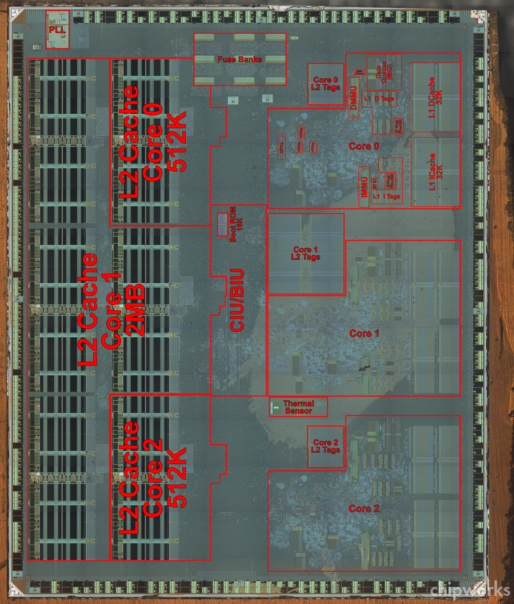
•Level 1 (L1) cache structure
•32 KB, 32-byte line, 8-way set-associative instruction cache
•32 KB, 32-byte line, 8-way set-associative data cache
•Single-cycle cache access
•Pseudo least-recently-used (PLRU) replacement
•Copy-back or write-through data cache (on a page-per-page basis)
•Supports PowerPC memory coherency modes
•Nonblocking instruction and data cache (supports hits under one outstanding miss)
•No snooping of instruction cache
•Memory management unit
•128 entry, 2-way set-associative instruction TLB
•128 entry, 2-way set-associative data TLB
•Hardware reload for TLBs
•Eight instruction block address translation (BAT) arrays and eight data BATs
•Virtual memory support for up to 4 petabytes (252) of virtual memory
•Real memory support for up to 4 gigabytes (232) of physical memory
•Level 2 (L2) cache
•256 KB, 64-byte line, 2-way set-associative on-chip cache memory
•Internal L2 cache controller with 2 K-entry tag array
•Copy-back or write-through data cache (on a page basis, or for all L2)
Datasheet
DD2.X
PowerPC 750CL Microprocessor
Version 2.6
October 16, 2009
General Information
Page 11 of 70
•64-byte cache line organized as two 32-byte sectors
•L2 frequency at core speed
•Selectable 32-byte, 64-byte, or 128-byte L2 cache loads
•Error correction code (ECC) protection on cache array
•Bus interface
•Compatible with the 60x processor interface
•Has a 32-bit address bus
•Has a 64-bit data bus (also supports 32-bit data bus mode)
•Supports bus-to-core frequency multipliers of 2x, 2.5x, 3x, 3.5x, 4x, 4.5x, 5x, 5.5x, 6x, 6.5x, 7x, 7.5x, 8x, 8.5x, 9x, 9.5x, and 10x
•Bus transaction pipeline depth of 2, 3, or 4 transactions (selectable)
•Testability
•Level sensitive scan design (LSSD)
•JTAG interface

")