• Hey, guest user. Hope you're enjoying NeoGAF! Have you considered registering for an account? Come join us and add your take to the daily discourse.

AMD Oberon PlayStation 5 SoC Die Delidded and Pictured

ReBurn

Gold Member
I'm shutting down console war nonsense. PS5 fanboys are doing the exact some nonsense Xbox fanboys did when it turned out the Xbox One was a less powerful system than the PS4 last time around. There's no secret sauces yet to be found, we have known the full specs of both systems for months/years at this point.
Lol ending console warring by console warring.
 

ethomaz

Banned
From my understanding it's like a mini version of infinity cache. What AMD does for their desktop GPUs takes up too much much and is expensive to boot. So in theory a slimmed down version would be possible on smaller chips.

To those that are offended. I'm not saying that the PS5 has infinity cache. I'm not that dumb.
Infinity Cache is actually configurable in size.
6800 has that big one but AMD said the smaller GPUs will have less.

For example RX 6600 has 32MB Infinty Cache only.
 
Last edited:

Zathalus

Member
The article says PS5’s GPU has L3 cache…. Is that really true?
The article says nothing of the sort.

There is a clear indication of AMD's Infinity Fabric, which connects the entire chip, and L2 cache. The GDDR6X memory controller and PHY (physical layer) interface can be seen on the edge of the SoC, which is where the data enters and exits the processor. Looking closely, you can see the L3 cache there as well.

It is referring to the L3 cache on the SoC, in other words, the CPU L3 cache, which is on the edge of the SoC next to the CPU clusters.
 

ethomaz

Banned
The article says nothing of the sort.


It is referring to the L3 cache on the SoC, in other words, the CPU L3 cache, which is on the edge of the SoC next to the CPU clusters.
"The GDDR6X memory controller and PHY (physical layer) interface can be seen on the edge of the SoC, which is where the data enters and exits the processor. Looking closely, you can see the L3 cache there as well."

They are clearly talking about L3 cache between the GDDR6X controller and PHY on the edge of the SoC.
Not the L3 cache on CPU that are more in the middle left of the chip far away from the GDDR6x and PHY lol
 
Last edited:

Xyphie

Member
EuNU-3oXMAIiJ6a


Fully annotated die shot from literally months ago, as any reasonable person can see there's no L3 cache for the GPU. The things inbetween the PHYs are interconnects (think highways for data transfer inside the chip).
 

Zathalus

Member
"The GDDR6X memory controller and PHY (physical layer) interface can be seen on the edge of the SoC, which is where the data enters and exits the processor. Looking closely, you can see the L3 cache there as well."

They are clearly talking about the GPU.
No they are not, they are referring to the SoC as a whole. The word GPU occurs before they even mention the CPU, with both occurring in the previous paragraph. The entire leading sentence refers to the SoC, hence SoC is the subject of both that and the following sentence. E.g L3 cache for the SoC, GDDR6X controller for the SoC, PHY for the SoC.
 

ethomaz

Banned
I wonder how people know what kind of cache it is just by looking at it.
Type? It is called L3 because it is a level higher than L2 that is higher than L1 that is higher than L0.
You start from the close to the core and each new level of cache receive a number.
There not that much diference in terms of silicon look between them.

So L3, L2, L1 is more related to the place/level of the cache.
 
Last edited:

ethomaz

Banned
No they are not, they are referring to the SoC as a whole. The word GPU occurs before they even mention the CPU, with both occurring in the previous paragraph. The entire leading sentence refers to the SoC, hence SoC is the subject of both that and the following sentence. E.g L3 cache for the SoC, GDDR6X controller for the SoC, PHY for the SoC.
Read again please lol
 

ethomaz

Banned
Please demonstrate where the word L3 and GPU are correlated in the article.
"The GDDR6X memory controller and PHY (physical layer) interface can be seen on the edge of the SoC, which is where the data enters and exits the processor. Looking closely, you can see the L3 cache there as well."

"there as well" = The place he is talking about... the edge of the SoC... the GDDR6x... the PHY... where the data enters and exits the processor.
 
Last edited:

Zathalus

Member
""The GDDR6X memory controller and PHY (physical layer) interface can be seen on the edge of the SoC, which is where the data enters and exits the processor. Looking closely, you can see the L3 cache there as well.""
The word GPU is not mentioned anywhere.
 

ethomaz

Banned
I can only conclude English is not your first language as this is pretty sad. SoC does not mean GPU.
That is what I'm guessing from you.
Lack of comprehension.

The phase is very clear... he direct pointed the place he is talking about.

"there as well" = The place he is talking about... the edge of the SoC... the GDDR6x... the PHY... where the data enters and exits the processor.

The CPU cache is not even close to that place.
 
Last edited:

MarkMe2525

Gold Member
This is really cool. Are people confusing infinity fabric with infinity cache? Also, does that and AMD 2019 stamp mean it was designed in 19 or actually fabricated?

Edit: that stamp was on a different chipset he imaged. I didn't realize I was going through all the shots he has done.
 
Last edited:

onesvenus

Member
That is what I'm guessing from you.
Lack of comprehension.

The phase is very clear... he direct pointed the place he is talking about.

"there as well" = The place he is talking about... the edge of the SoC... the GDDR6x... the PHY... where the data enters and exits the processor.

The CPU cache is not even close to that place.
Can you point in an image where you think the CPU and GPU L3 $s are? I think that would easily guide the discussion instead of reposting the same quote over and over again
 

ethomaz

Banned
Can you point in an image where you think the CPU and GPU L3 $s are? I think that would easily guide the discussion instead of reposting the same quote over and over again
I posted twice in the tread.
It is not me… it come from the article.


That is the cache the article is claiming.
CPU cache is between the CPU cores in the left of the pic.

That pic probably helps to find the CPU cache (purple).

EuNU-3oXMAIiJ6a


The article is talking about that gray part near the GDDR6x controller.
 
Last edited:

MarkMe2525

Gold Member
No.
The PS5 and Series X|S silicon have stamped 2019 like all AMD processors.
I stand corrected, that was from the ps5 soc. Since you brought the series consoles up, I cannot for the life of me find series x die shot that is this close and detailed. Would you happen to know where some of those are? Not that I would be able to make heads or tails of what I'm looking at.
 
There is a difference in that there are quite a few examples of the PS5 outperforming the XSX at least in terms of framerate. But I know many will just say that is because of MS lacklustre tools.
The ship has sailed on this kind of stuff. The PS5 does better in framerates sometimes because it's often running at clearly inferior resolutions. There were odd early cases at the start of the gen, but those cases are rapidly drying up. There are plenty more examples of games where Series X boasts superior resolution as well as matching or superior framerate performance.

If the PS5 is running at clearly inferior resolutions and Series X has better or matching performance the PS5 isn't actually the one performing better.
 
Last edited:

ethomaz

Banned
I stand corrected, that was from the ps5 soc. Since you brought the series consoles up, I cannot for the life of me find series x die shot that is this close and detailed. Would you happen to know where some of those are? Not that I would be able to make heads or tails of what I'm looking at.
The only die shot I have is the one MS shared.
About the stamps a Chinese site reveled all of them early this year but I’m having a hard time to find them side the lack of Chinese skills… I’m trying to find the link here in GAF but it is being hard to find the link.

AMD stamps are when the final chip was designed/finalized.
 
Last edited:
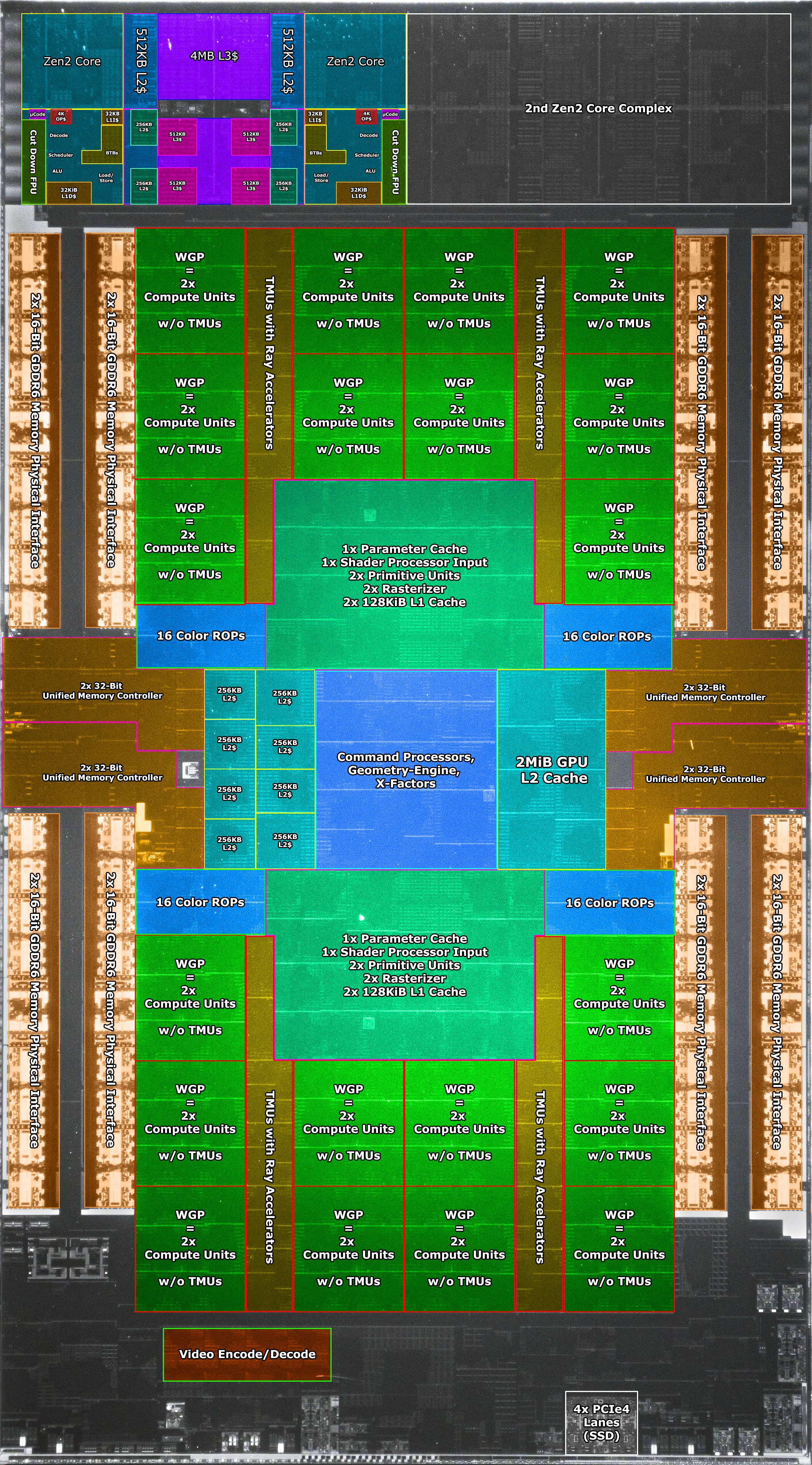
Ah, there's a bit of confusion because that was two rumored "secret sauces" that Cerny in his infinite wisdom had chosen from AMD's roadmap that would help the PS5 perform much higher than its variable CPU and 10TF, both involving L3.
One was Zen3's unified cache that ended not happening and L3 cache for the GPU, that it looks like it happened but by an irrelevant degree.


I'm shutting down console war nonsense. PS5 fanboys are doing the exact some nonsense Xbox fanboys did when it turned out the Xbox One was a less powerful system than the PS4 last time around. There's no secret sauces yet to be found, we have known the full specs of both systems for months/years at this point.

The situation is actually the inverse! The "second GPU" does actually exists here!

The thing that people should take away from all this is that all these little features that each company puts on their machines helps little and may makes little difference in practice all things considered.
IF helps achieve a higher effective bandwidth, but can't the same be achieve by a more traditional way, just using more memory channels or faster memory? The amount of IF there is very small so in practice we can't think like if the PS5 have more effective bandwidth than the SEX (but is should help with latency, that was none of Cerny's goals?).
 
Please ethomaz ethomaz stop while you still can. There is not L3 cache for GPU, only for CPU.


I WANT TO SCREAM!
Infinite Cache is L3 cache! If is just a marketing name AMD made up, like they tried to do with Zen2/3 L3 calling it GameCache!

I understand people not wanting to accept, but the discussing is still not closed! With the new dieshots those unknow structures are looking more like cache than it looked before and it's exactly in the right place.
And if it is, so what, Xboxers?! Makes no difference for you, the SeX loses nothing because like I explained the practical difference is small and the performance is influenced by many other factors! The SeX has things that the PS5 does not, deal with it.
 
Last edited:

MarkMe2525

Gold Member
The only die shot I have is the one MS shared.
About the stamps a Chinese site reveled all of them early this year but I’m having a hard time to find them side the lack of Chinese skills… I’m trying to find the link here in GAF but it is being hard to find the link.

AMD stamps are when the final chip was designed/finalized.
Thanks for the info
 

ANDS

King of Gaslighting
I can't read that headline as anything other than "Dediddled and pictured. . ."

. . .what's the TLDR for the dopes among us so we can be properly impressed (or disappointed?) -
 
So, it DOES have L3 cache after all..
Lmfaoo
Uh, yeah? The CPU always had L3$, that's a staple of AMD processors (and just modern processors in general, except maybe Pi-like devices). Was there ever folks saying it didn't?

I found the pic on the gallery of the supposed L3 cache:


Is that confirmed to be the L3$? If so it'd appear it's unified.

And yes I'm just referring to CPU.
 
Last edited:


What he says there is true, but apparently Control was a poor use-case because its issues on Series, according to DF, were system OS-related. A recent system update seemed to "automatically" bump up performance greatly for the game on that platform.

Which I think just further goes to show what role OS resources and optimizations also can play in performance peaks and stability. Returnal had vaguely similar issues but in regards to data integrity with suspended states being lost due to, in Housemarque's words, system-related OS issues.

Not sure if those have been cleared up yet but yeah, just more examples there.
 

Zathalus

Member
That is what I'm guessing from you.
Lack of comprehension.

The phase is very clear... he direct pointed the place he is talking about.

"there as well" = The place he is talking about... the edge of the SoC... the GDDR6x... the PHY... where the data enters and exits the processor.

The CPU cache is not even close to that place.
Yes, the statement is referring to the edge of the SoC. Which has four sides. Which just so happens to have one side that has the L3 cache for the CPU clusters.
 

Garani

Member
The ship has sailed on this kind of stuff. The PS5 does better in framerates sometimes because it's often running at clearly inferior resolutions. There were odd early cases at the start of the gen, but those cases are rapidly drying up. There are plenty more examples of games where Series X boasts superior resolution as well as matching or superior framerate performance.

If the PS5 is running at clearly inferior resolutions and Series X has better or matching performance the PS5 isn't actually the one performing better.
Aren't we salty today?

Don't worry, no one will take away your favorite plastic box.
 
Top Bottom