That there's a difference in die size at all is all the evidence you need to see these are independent products. If that isn't obvious to you, you're clearly not informed enough on the subject matter at hand.
They are well rebinned/obsolete/anything else based products that look very
similar to an original Xbox One APU. i am not going to be daft and ignore that there
is a difference whatsoever. And to be frank, prior to any of the mentioned sources, this
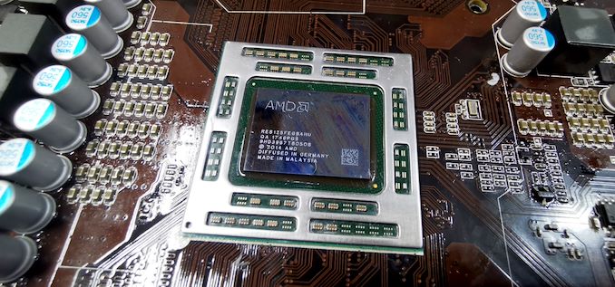
thing for lack of a better word was confusing as all hell. It can clock itself to Xbox One X CPU speeds. Its GPU was mentioned by Chuwi as an R7 350, even though it clearly is not a R7 350. Its die looking incredibly similar
but not one for one the same is confusing (And raised suggestion that it was, perhaps, a revision)? Heck, early one it was suggested that there was a
seperate, discrete GPU outside the APU under a different cooler.
From the random nature of the quality of the drivers to the completely random quality of the motherboards that are provided in the dozen's, this thing has a crapton going for it that just confuses the heck. Hell even Anandtech came up with a memory speed for the DDR3 modules and GPU that made little sense (Dual channel when the entire APU seems designed for quad channel) and TCC had incredible difficulties getting a memory configuration that would actually
work.
To put short, this entire APU makes no sense.
Having said that, I don't see why you have to tell me that i am not informed enough in such an antagonizing way. You again state that the die size alone is enough of a difference to cast doubt on whether or not its an actual Xbox One APU. Given the confusing nature of the chip itself, that'' understandable. But do you have any source that provides additional evidence to your doubt that it is a fully independent product? That's what i am after. I am not denying that the die sizes are the same, mind you.
I fully buy into the theory that the XBO APU was/is used as a blueprint for a very similar looking APU, but i'd love to read verification on that. One aspect that helps your point of doubt is the fact that it uses an absolutely ancient procede - 28nm. AMD has been known to release
new processors on super old procedes, of which the A9-9820 may very well be one.
Again, on the removal of eSRAM, you're failing to understand the fine grained intricacies of the design of on-die comms, control and I/O circuitry. It's not a software issue but a hardware design one. You cannot just take an APU chip with a GPU archetected around writing its framebuffer to an eSRAM scratchpad (designed specifically to accomodate the precise bandwidth and latency requirements) and just disable/fuse the eSRAM and hope for any reasonable GPU performance.
I don't absolutely believe its just a flick of a switch, obviously. But in a rational fashion, for it to use ESRAM would mean you either have Windows driver support for it, or tread it in the same way Intel did with CrystalWell - As a seperate cache recognized at the hardware level. The latter may very well be true, but nothing to date so far supports that.
To your other points you argued previously about serial numbers suggesting a date of manufacture of this new chip, it's merely circumstantial at best. AMD made a lot of products in 2013, does that mean they're also XB1 APUs? Your reasoning doesn't follow sound logic.
True, but how many products by AMD made in 2013 were an octacore Jaguar part? The best one could come up with is either an XBO APU or a completely unknown part based off two Athlon 53xx modules. I don't consider the latter a realistic possibility (Crafting a completely new processor, unknown to the public for several years to then appear in a obscure machine made for Asian customers?). Logical deduction would rather suggest the former, that its an Xbox One APU or some offshoot of it (Anandtech does call it an
Durango+ for a reason)
What makes your reasoning sound more logic, then.
Also, i'm pretty baffled by your sheer refusal to acknowledge the possibility that three independent tech media outlets can all be wrong, when they consistently are so often, especially given their obvious lack of domain knowledge, as evidenced by their naive claims that a chip with totally different memory subsystem design and clearly different die size is the same as another, simply because the CPU and GPU core counts align. It's misinformed at best and at worst, just plain ignorant.
See the above. I think they can all be wrong given the confusing nature of the chip itself. However, they have provided quite a lot of evidence to back up what they write in words. By comparison, you disagree in full by stating a single point of argument - The die size.
Which, okay, is different, and can very well be reason its an off shoot. But are there outlets stating the same thing? Are there outlets taking screencaps/dieshots/dismantlements to reveal the inner details? That's what i am after.